Heterostructure-enabled Photonic Devices
Assembling materials with different electrical, optical and magnetic properties into heterostructures represent a highly flexible route to tackle some of the challenges facing today’s nanoelectronics and optoelectronics. Admittedly, the fabrication of high-performance heterostructure devices is becoming one major line of research in the field of nanotechnology and materials sciences.
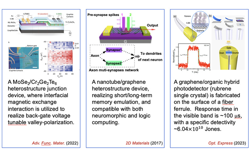
Photosensitive devices play a major role in today’s ICT systems and their functionalities are constantly evolving as driven by the needs to achieve still greater integration, broader spectral coverage, faster response, and more recently smarter operation. In 2015, we proposed and demonstrated for the first time an all-carbon strategy for graphene-based photodetectors, combining mixed-dimensional carbon allotropes. The devices feature facile fabrication, robust operation, and can be easily processed into flexible devices. Our group keeps exploring new concept devices based on low-dimensional semiconductor heterostructures, and the following list some exemplar research output in this area of our efforts.
Related group publications:
Nature Comm. 6, 9589 (2015) Nanoscale 8, 12883 (2016) Nano Research 10, 1880 (2017) Carbon 146, 486 (2019) Carbon 167, 668 (2020) | Adv. Func. Mater. 2204779 (2022) Adv. Science 2204332 (2022) ACS Appl. Mater. Inter.13, 57735 (2021) ACS Appl. Mater. Inter. 10, 38326 (2018) 2D Materials 4, 035022 (2017) |